- 您现在的位置:买卖IC网 > Sheet目录315 > BD6581GU-E2 (Rohm Semiconductor)IC LED DVR WHT BCKLGHT VCSP85H2
BD6581GU
Datasheet
● The Coil Selection
The DC/DC is designed by more than 4.7μH. When L value sets to a lower value, it is possibility that the specific
sub-harmonic oscillation of current mode DC / DC will be happened. Please do not let L value to 3.3μH or below.
And, L value increases, the phase margin of DC / DC becomes to zero. Please enlarge the output capacitor value when you
increase L value.
Example)
4.7μH = output capacitor 2.2μF/50V 1pcs
6.8μH = output capacitor 2.2μF/50V 2pcs
10μH = output capacitor 2.2μF/50V 3pcs
This value is just examples, please made sure the final judgment is under an enough evaluation.
● Layout
In order to make the most of the performance of this IC, its layout pattern is very important. Characteristics such as
efficiency and ripple and the likes change greatly with layout patterns, which please note carefully.
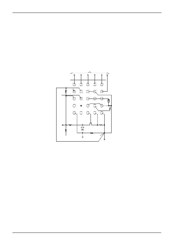
to Anode of each LED
E
LED6
LED5
LED4
LED3
LED2
Reset
C BAT
D
PWM
RSTB
GND
FAILSEL
GND
LED1
C
C REG
VBAT
PWMPOW
VREG
ISETL
PWMDRV
B
A
TEST
ISETH
GND
VDET
SW
SENSP
SENSN
1
2
3
4
5
Tr
C IN
L
SBD
C OUT
R SENSE
to Cathode of LED
to GND
Figure 40. Layout
Connect the input bypath capacitor CIN(10μF) nearest to coil L, as shown in the upper diagram.
Wire the power supply line by the low resistance from CIN to VBAT pin. Thereby, the input voltage ripple of the IC can be
reduced. Connect smoothing capacitor CREG of the regulator nearest to between VREG and GND pin, as shown in the
upper diagram. Connect schottky barrier diode SBD of the regulator nearest to between coil L and switching transistor Tr.
And connect output capacitor COUT nearest to between CIN and GND pin. Thereby, the output voltage ripple of the IC can
be reduced.
Connect switching transistor Tr nearest to SW pin. Wire coil L and switching transistor Tr, current sensing resistor R SENSE by
the low resistance. Wiring to the SENSP pin isn't Tr side, but connect it from R SENSE side. Over current value may become
low when wiring from Tr side. Connect R SENSE of GND side isolated to SENS pin. Don’t wire between R SENSE and SNESN
pin wiring from R SENSE pin to GND pin. And R SENSE GND line must be wired directly to GND pin of output capacitor. It
has the possibility that restricts the current drive performance by the influence of the noise when other GND is connected to this
GND.Connect LED current setting resistor RISET nearest to ISET pin. There is possibility to oscillate when capacity is
added to ISET terminal, so pay attention that capacity isn't added. And, RISET of GND side must be wired directly to
GND pin. When those pins are not connected directly near the chip, influence is given to the performance of BD6581GU,
and may limit the current drive performance. As for the wire to the inductor, make its resistance component small so as to
reduce electric power consumption and increase the entire efficiency.
www.rohm.com
? 2012 ROHM Co., Ltd. All rights reserved.
TSZ22111 ? 15 ? 001
20/32
TSZ02201-0G3G0C400170-1-2
03.Dec.2012 Rev.001
发布紧急采购,3分钟左右您将得到回复。
相关PDF资料
BD6583MUV-AE2
IC LED DRIVER WHIT BCKLGT 24VQFN
BD6586MUV-E2
IC LED DRVR WHITE BCKLGT 24-VQFN
BD6592MUV-E2
IC LED DRVR WHITE BCKLGT 24-VQFN
BD7844AEFV-E2
IC LED DISPLAY DVR 5V 28-HTSSOP
BD8105FV-E2
IC LED DVR SERIAL PAR 20-SSOP
BD8112EFV-ME2
IC LED DRIVER 24-VSSOP
BD8119FM-ME2
IC WHITE LED DVR PWM 28-HSOP
BD82103GWL-E2
IC LED DRVR WHITE BCKLGT 11-UCSP
相关代理商/技术参数
BD6583MUV
制造商:ROHM 制造商全称:Rohm 功能描述:Step-up DC/DC converter for medium size LCD panel
BD6583MUV-A
制造商:ROHM 制造商全称:Rohm 功能描述:White Backlight LED Driver for Medium to Large LCD Panels (Switching Regulator Type)
BD6583MUV-A_11
制造商:ROHM 制造商全称:Rohm 功能描述:White Backlight LED Driver for Medium to Large LCD Panels (Switching Regulator Type)
BD6583MUV-AE2
功能描述:IC LED DRIVER WHIT BCKLGT 24VQFN RoHS:是 类别:集成电路 (IC) >> PMIC - LED 驱动器 系列:- 标准包装:60 系列:- 恒定电流:- 恒定电压:- 拓扑:线性(LDO),PWM,升压(升压) 输出数:8 内部驱动器:是 类型 - 主要:背光 类型 - 次要:RGB,白色 LED 频率:500kHz ~ 1.5MHz 电源电压:4.75 V ~ 26 V 输出电压:45V 安装类型:* 封装/外壳:* 供应商设备封装:* 包装:* 工作温度:-40°C ~ 85°C
BD6583MUV-E2
功能描述:LED照明驱动器 72 LEDs 2.7-22V 43V Max Out 25mA Out RoHS:否 制造商:STMicroelectronics 输入电压:11.5 V to 23 V 工作频率: 最大电源电流:1.7 mA 输出电流: 最大工作温度: 安装风格:SMD/SMT 封装 / 箱体:SO-16N
BD6586MUV
制造商:ROHM 制造商全称:Rohm 功能描述:Silicon Monolithic Integrated Circuit
BD6586MUV_11
制造商:ROHM 制造商全称:Rohm 功能描述:White Backlight LED Driver for Medium to Large LCD Panels (Switching Regulator Type)
BD6586MUV-E2
功能描述:LED照明驱动器 24 LEDs 2.7-5.5V 24V Max Out 25mA Out RoHS:否 制造商:STMicroelectronics 输入电压:11.5 V to 23 V 工作频率: 最大电源电流:1.7 mA 输出电流: 最大工作温度: 安装风格:SMD/SMT 封装 / 箱体:SO-16N
